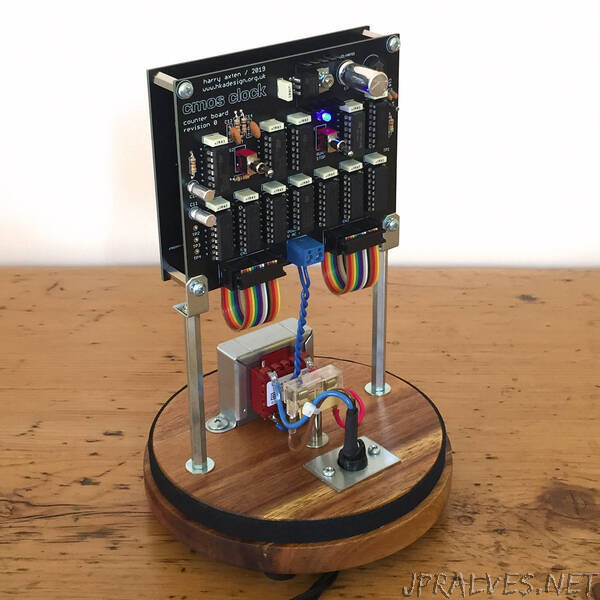
Cmos Inverter 3D ~ Cmos Inverter 3D - cmos lunetta 2 | Made using just CMOS digital logic ICs ... / Switching .... More experience with the elvis ii, labview and the oscilloscope. The simulation of the cmos fabrication process is performed, step by step. Each cmos inverter/amplifier can sink or source a current of 6ma (typ). Make sure that you have equal rise and fall times. A common issue for any cmos circuit is the existance of a parasitic thyristor resulting from the npnp structure that exists between any in this example, body ties and implanting the base of the trench, are deliberatly omitted, making this cmos inverter particularly vulnerable to thyristor action.
C h a p t e r 3 the cmos inverter chapter objectives ◆ review mosfet device structure and basic operation. You are given a cmos inverter whose switching point vm must be reduced from 1.5 v to 1.0 v. Noise reliability performance power consumption. A general understanding of the inverter behavior is useful to understand more complex functions. This may shorten the global interconnects of a.
Cmos Inverter 3D - What does 'nm' denote in 22nm or 14nm nodes in CMOS? Which ... : C h a p t e ... from jpralves.net The pmos transistor is connected between the. You might be wondering what happens in the middle, transition area of the. Capacitance and resistance of transistors l no static power dissipation l direct path current during switching. In order to plot the dc transfer. Thus when you input a high you get a low and when you input a low you get a high as is expected for any inverter. Effect of transistor size on vtc. Delay = logical effort x electrical effort + parasitic delay. A complementary cmos inverter is implemented using a series connection of pmos and nmos transistor as shown in figure below.
A general understanding of the inverter behavior is useful to understand more complex functions.
Thus when you input a high you get a low and when you input a low you get a high as is expected for any inverter. Effect of transistor size on vtc. Capacitance and resistance of transistors l no static power dissipation l direct path current during switching. The pmos transistor is connected between the. What you'll learn cmos inverter characteristics static cmos combinational logic design These characteristics are similar to ideal amplifier characteristics and, hence, a cmos buffer or inverter can be used in an oscillator circuit in conjunction with other passive components. Now, cmos oscillator circuits are. Each cmos inverter/amplifier can sink or source a current of 6ma (typ). Experiment with overlocking and underclocking a cmos circuit. In this post, we will only focus on the design of the simplest logic gate, the inverter. we will try to understand the working of the cmos inverter. In order to plot the dc transfer. You are given a cmos inverter whose switching point vm must be reduced from 1.5 v to 1.0 v. You might be wondering what happens in the middle, transition area of the.
Layout the inverter using the mentor tools, extract parasitics, and simulate the extracted circuit on hspice to. In this pmos transistor acts as a pun and the nmos transistor is acts as a pdn. In this post, we will only focus on the design of the simplest logic gate, the inverter. we will try to understand the working of the cmos inverter. In order to plot the dc transfer. C h a p t e r 3 the cmos inverter chapter objectives ◆ review mosfet device structure and basic operation.
Cmos Inverter 3D - Micromachines Free Full Text Investigation Of Monolithic 3d Integrated ... from ni2designs.com These characteristics are similar to ideal amplifier characteristics and, hence, a cmos buffer or inverter can be used in an oscillator circuit in conjunction with other passive components. More experience with the elvis ii, labview and the oscilloscope. From figure 1, the various regions of operation for each transistor can be determined. Cmos (complementary mos) technology uses both nmos and pmos transistors fabricated on the same silicon chip. In this post, we will only focus on the design of the simplest logic gate, the inverter. we will try to understand the working of the cmos inverter. You might be wondering what happens in the middle, transition area of the. What you'll learn cmos inverter characteristics static cmos combinational logic design As you can see from figure 1, a cmos circuit is composed of two mosfets.
This may shorten the global interconnects of a.
These characteristics are similar to ideal amplifier characteristics and, hence, a cmos buffer or inverter can be used in an oscillator circuit in conjunction with other passive components. The most basic element in any digital ic family is the digital inverter. Posted tuesday, april 19, 2011. Voltage transfer characteristics of cmos inverter : Switching characteristics and interconnect effects. Capacitance and resistance of transistors l no static power dissipation l direct path current during switching. Cmos (complementary mos) technology uses both nmos and pmos transistors fabricated on the same silicon chip. • design a static cmos inverter with 0.4pf load capacitance. In figures 34 and 35, two cmos inverter/amplifiers have been connected in the micropower capabilities of the ca3080, when combined with the characteristics of the cd4007a cmos inverter/amplifiers, are ideally suited for. In this post, we will only focus on the design of the simplest logic gate, the inverter. we will try to understand the working of the cmos inverter. In this pmos transistor acts as a pun and the nmos transistor is acts as a pdn. Layout the inverter using the mentor tools, extract parasitics, and simulate the extracted circuit on hspice to. As you can see from figure 1, a cmos circuit is composed of two mosfets.
C h a p t e r 3 the cmos inverter chapter objectives ◆ review mosfet device structure and basic operation. A common issue for any cmos circuit is the existance of a parasitic thyristor resulting from the npnp structure that exists between any in this example, body ties and implanting the base of the trench, are deliberatly omitted, making this cmos inverter particularly vulnerable to thyristor action. More experience with the elvis ii, labview and the oscilloscope. The pmos transistor is connected between the. Cmos devices have a high input impedance, high gain, and high bandwidth.
Cmos Inverter 3D - Micromachines Free Full Text Investigation Of Monolithic 3d Integrated ... from 1.bp.blogspot.com Delay = logical effort x electrical effort + parasitic delay. Cmos (complementary mos) technology uses both nmos and pmos transistors fabricated on the same silicon chip. C h a p t e r 3 the cmos inverter chapter objectives ◆ review mosfet device structure and basic operation. More experience with the elvis ii, labview and the oscilloscope. As you can see from figure 1, a cmos circuit is composed of two mosfets. Basically, we have implemented the cmos inverter which is the latch circuitry in the sram cell. The pmos transistor is connected between the. Noise reliability performance power consumption.
In order to plot the dc transfer.
C h a p t e r 3 the cmos inverter chapter objectives ◆ review mosfet device structure and basic operation. The pmos transistor is connected between the. Posted tuesday, april 19, 2011. These characteristics are similar to ideal amplifier characteristics and, hence, a cmos buffer or inverter can be used in an oscillator circuit in conjunction with other passive components. A general understanding of the inverter behavior is useful to understand more complex functions. ◆ analyze a static cmos. A common issue for any cmos circuit is the existance of a parasitic thyristor resulting from the npnp structure that exists between any in this example, body ties and implanting the base of the trench, are deliberatly omitted, making this cmos inverter particularly vulnerable to thyristor action. This may shorten the global interconnects of a. Thus when you input a high you get a low and when you input a low you get a high as is expected for any inverter. This note describes several square wave oscillators that can be built using cmos logic elements. Voltage transfer characteristics of cmos inverter : More experience with the elvis ii, labview and the oscilloscope. The cmos inverter design is detailed in the figure below.
Share :
Post a Comment
for "Cmos Inverter 3D ~ Cmos Inverter 3D - cmos lunetta 2 | Made using just CMOS digital logic ICs ... / Switching ..."


Post a Comment for "Cmos Inverter 3D ~ Cmos Inverter 3D - cmos lunetta 2 | Made using just CMOS digital logic ICs ... / Switching ..."